
Making printed circuit boards
Making a printed circuit board: a marker, toner transfer and photoresist, etching in ferric chloride, drilling, safety, and ordering boards.
Only make a board with an adult present
Making a board needs corrosive chemicals, a hot iron and a drill. Children make boards only with an adult, who supervises the whole time, prepares and puts away the chemicals, and handles the hot and sharp tools. Before you start, read this whole page and the instructions on the chemicals' packaging together.
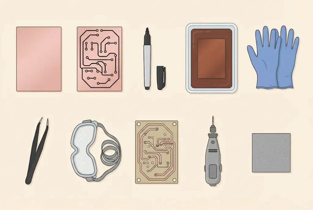
- Protection: nitrile gloves, safety glasses and old clothes or an apron. The etching solution permanently stains skin, clothes, wood and sinks.
- Space: work with a window open or outdoors, on a surface you are allowed to stain. Don't breathe the fumes.
- Containers: plastic or glass only, and plastic tweezers. The solution eats metal. Containers and tools you use for chemicals are never used for food again.
- If the solution gets on your skin, rinse it off with plenty of water. If it gets in your eye, rinse the eye under running water for at least 15 minutes and see a doctor.
- Don't heat the solution above 50 °C, never on a cooker or in a microwave, and don't mix it with other chemicals.
- Don't pour it down the drain. Used solution contains dissolved copper, which is poisonous to life in water. Take it to a recycling centre as hazardous waste.
- Acetone and alcohol catch fire easily: keep them away from flames and the hot iron.
- The dust from drilling and cutting a glass-fibre board irritates the skin and lungs. Don't blow it away; wipe it up with a damp cloth.
- Keep the chemicals in their original, labelled packaging, locked away from children. Never pour them into a drinks bottle.
What is a printed circuit board?
A printed circuit board (PCB) is a board of insulating material with copper tracks on it instead of wires. Components go into holes and are soldered to the copper, so they can’t work loose as on a breadboard.
A board is made from a sheet covered in copper. The sheet is usually FR4, glass fibre in epoxy resin, 1.6 mm thick, and the copper on it is only 35 µm (35 thousandths of a millimetre) thick. A cheaper FR2 sheet is made of paper and resin: it is easier to drill but less strong.
The idea is simple: we cover the copper with a protective layer where the tracks should be, and dissolve the rest of the copper.
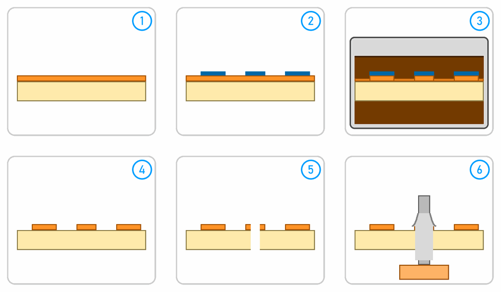
- Clean the copper-clad sheet.
- Transfer the board’s drawing onto the copper as a protective layer: with a marker, with toner from a laser printer, or by the photo method.
- Put the board into the etching solution. The solution eats away and dissolves the bare copper, and the copper under the protective layer stays.
- Remove the protective layer. The copper tracks are left.
- Drill the holes for the leads.
- Fit and solder the components.
The board’s drawing
You can make the drawing with a pencil on squared paper or in KiCad, a free program. For a hand-made board, use:
- tracks at least 0.5 mm wide, and at least 1 mm for a marker,
- gaps between tracks and pads of at least 0.5 mm,
- pads (round copper areas round the holes) at least 2 mm across, with a small hole in the middle that later guides the drill.
For tracks that carry a large current, see How much current a track can carry.
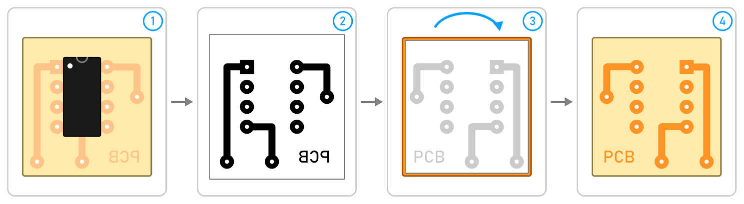
Watch out for mirroring. On a single-sided board the components are on top and the copper underneath. When you turn the board over to look at the copper, everything is mirrored: a chip with pin 1 at the top left now has pin 1 at the top right. With toner transfer and the photo method, you put the paper or film on the copper face down, so the drawing is mirrored once more. That is why in KiCad you print the bottom copper layer unmirrored and the top layer mirrored. The safest way is to add a short piece of text to the copper layer: on the finished board it must read correctly when you look at the copper side.
Preparing the board
- Cut the board to size: score it several times on both sides along a ruler with a craft knife and snap it over the edge of a table, or cut it with a hacksaw. An adult holds the tool, and the dust is wiped up with a damp cloth.
- Clean the copper with the rough side of a kitchen sponge or fine steel wool and a drop of washing-up liquid, until it is evenly shiny. Rinse it with water and dry it.
- Don’t touch the copper with your fingers any more. Grease from your fingers stops the etching, so copper is left in that spot.
Three ways to transfer the drawing
| Marker | Toner transfer | Photo method | |
|---|---|---|---|
| Thinnest track | about 1 mm | about 0.4 mm | about 0.2 mm |
| What you need | a waterproof marker | a laser printer, glossy paper, an iron | a photoresist board, film, a UV lamp, developer |
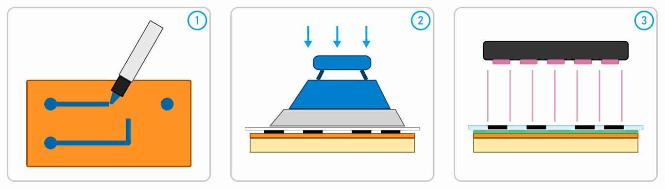
| Good for | a first board, a simple circuit | most boards | fine tracks and chips |
1. A marker
The simplest way. A waterproof marker (for CDs or for labelling) covers the copper with a layer of ink that protects it from the solution. Not every marker protects well, so try yours on a scrap of board first.
- Draw the layout in pencil, or transfer it by pricking through the paper (mark the pads with a needle).
- Draw the pads as dots first, then the tracks between them.
- When it is dry, go over everything a second time.
- Scrape off mistakes with a toothpick.
2. Toner transfer
The toner in a laser printer is a plastic powder that melts when it is heated. The iron moves it from the paper onto the copper. An inkjet printer doesn’t work, because ink isn’t plastic.
- Print the drawing with a laser printer on glossy paper (a page from a catalogue or magazine, or special transfer paper), at actual size (100 %) and with the darkest toner setting.
- Lay the paper toner side down on the cleaned copper.
- An adult presses the paper with an iron at its hottest setting (cotton, no steam) for 3 to 5 minutes, moving it slowly. Instead of an iron you can use a laminator and pass the board through it 5 to 10 times.
- Let the board cool, then soak it in lukewarm water with a drop of washing-up liquid for 10 to 20 minutes.
- Carefully rub the paper off the board with your fingers. The toner stays on the copper.
- Inspect the tracks. Fix any gaps with a marker.
3. The photo method
A photoresist board is a copper-clad board covered with a thin layer that changes under UV light (photoresist). With positive photoresist, the part that was lit dissolves later in the developer, and the part that wasn’t lit stays and protects the copper. A photoresist board is kept in the dark, in its packaging.
- Print the drawing on transparent film, tracks in black, as dark as possible. If the black is weak, print two films and lay one on top of the other.
- In dim light, peel the protective film off the board. Lay the film with the drawing on it, printed side towards the board, and press it down with a sheet of glass.
- Light the board with a UV lamp. The exposure time depends on the lamp and the board: find it with a test on a scrap of board or from the maker’s instructions.
- An adult mixes the developer following the board maker’s instructions. The developer is usually a solution of sodium hydroxide, which harms skin and eyes just like the etching solution: gloves and glasses are a must.
- Put the board into the developer and rock it gently. Within a minute or two the lit layer dissolves and the tracks appear. Rinse the board with water.
Etching in ferric chloride
A ferric chloride (iron(III) chloride, FeCl₃) solution is a dark brown liquid that dissolves copper. You buy it ready-made or as granules that you dissolve in water following the instructions on the packaging. The solution heats up while the granules dissolve: add the granules to the water slowly, a little at a time, and never pour water onto the granules.
Before you start, get everything together in one place: the tray, the tweezers, the board, a bowl of water for rinsing and an old cloth.
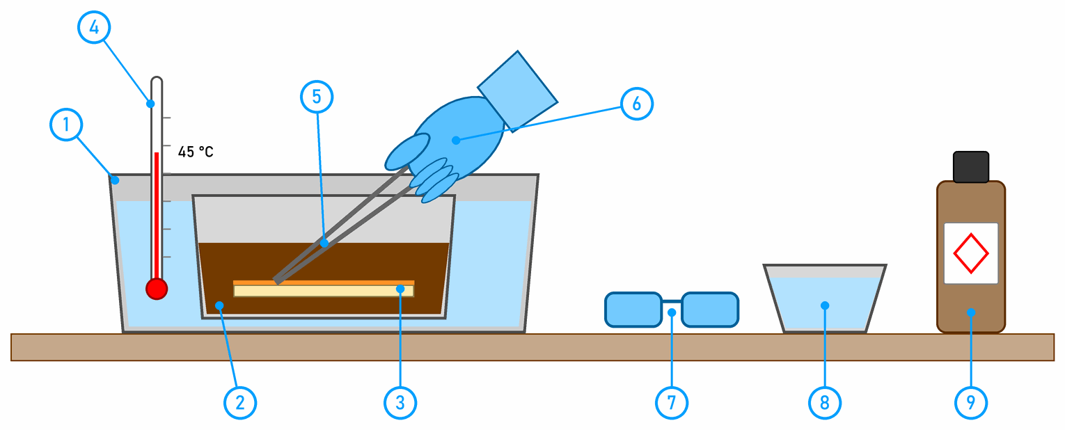
- Pour the solution into a plastic tray, enough to cover the board by a centimetre or two.
- The solution works faster when it is warm. Stand the tray of solution in a larger tray of warm water (up to 50 °C). Never heat it directly.
- With plastic tweezers, lower the board into the solution, copper side up.
- Rock the tray gently, so the solution flows over the copper.
- Check the board every few minutes. The copper disappears first at the edges. When the bare copper has gone everywhere, take the board out at once. Etching takes 10 to 30 minutes, less in a warm, fresh solution and more in a cold, used one.
- Rinse the board in the bowl of water, then under running water.
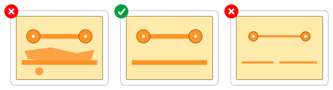
- Left: the board came out too early. Copper is left between the tracks and joins them. Put it back into the solution for a few minutes.
- Middle: good. The bare copper has gone everywhere, and the tracks are whole.
- Right: the board was in the solution too long. The solution has eaten into the tracks from under the protective layer, so they are thinner, and the thin ones have broken.
In chemical terms, ferric chloride takes copper into solution: 2 FeCl₃ + Cu → 2 FeCl₂ + CuCl₂. The more copper is dissolved, the slower the solution works, and it turns from brown to a dark greenish colour.
What do you do with the solution afterwards? The same solution can be used many times. Keep it in a plastic bottle with a lid and a clear label, locked away from children. When etching becomes very slow, take it, together with the water from the first rinse, to a recycling centre as hazardous waste. Never pour it down the drain: the copper in it is poisonous to fish and life in water, and the solution eats metal pipes.
Removing the resist, drilling and soldering
- Remove the protective layer with cotton wool and acetone (gloves, window open, away from flames) or with fine steel wool. The copper becomes shiny.
- Drill the holes with a small drill on a stand: a 0.8 mm bit for resistors, chips and most leads, 1.0 mm for pin headers and diodes, 1.2 to 1.5 mm for screw terminals and larger parts. Clamp the board, wear safety glasses, and lower the bit slowly: thin bits break easily. The small hole in the middle of each pad guides the bit to the right spot.
- Protect the copper from oxidising: coat it with solderable lacquer (rosin dissolved in alcohol) or cover the tracks with a thin layer of solder.
- Solder the components, from the lowest to the tallest (see Soldering).
- Check the board before you switch it on for the first time (see Troubleshooting a circuit).
How much current a track can carry
This part is for the Arduino workshop (ages 12 and up).
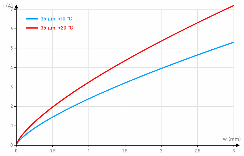
A track has a small resistance, so it warms up when current flows through it. How much current may flow is worked out with the IPC-2221 standard, from the track’s cross-section and how much it may warm up. For an outer track of 35 µm copper warming by 10 °C:
| Track width | Current |
|---|---|
| 0.5 mm | 1.5 A |
| 1 mm | 2.4 A |
| 2 mm | 4 A |
A 0.5 mm track is enough for signals, and power and coils, which draw several amps, need tracks of 1.5 to 2 mm. If there is room, make the track wider: a wide track costs nothing.
Ordering boards
You can also order a board drawn in KiCad from a PCB factory, such as JLCPCB and PCBWay (China), Aisler (Germany) or OSH Park (USA). A board like that has things that are hard to make at home:
- copper on both sides and holes with copper through them (plated holes), so tracks can move from one side to the other,
- a green solder mask that solder doesn’t stick to, so there are far fewer bridges,
- printed labels and component markings,
- tracks as narrow as 0.15 mm and accurately drilled holes.
How to order:
- In KiCad, check the design (the Design Rules Checker) and fix all errors.
- Export the Gerber files (a drawing of each layer) and the drill file, and pack them into one ZIP file. The factories have instructions for KiCad on their websites.
- Upload the ZIP file to the factory’s website and look at the board in their viewer: are all the layers and holes in place?
- Choose the number of layers (2), the thickness (1.6 mm), the colour and the quantity. Factories usually make at least 5 boards.
The boards are cheap, and the postage often costs more than they do. For parcels from outside the European Union you also pay VAT, and sometimes customs duty. Delivery takes one to three weeks. The order, the account on the factory’s website and the payment are handled by an adult.
| Made at home | Ordered | |
|---|---|---|
| Time | a few hours | one to three weeks |
| Copper sides | one | two or more |
| Solder mask and labels | no | yes |
| Thinnest track | 0.2 to 1 mm | 0.15 mm |
| Chemicals at home | yes | no |
| Best for | one board, a quick test | several boards, complex boards |
 What did we learn?
- A board is made only with an adult present, with gloves and glasses, and with a window open.
- We protect the copper where the tracks go with a marker, toner or the photo method, and dissolve the rest in ferric chloride.
- The board comes out of the solution as soon as the bare copper has gone: too early leaves copper between the tracks, too late thins the tracks.
- We never pour the solution down the drain; it goes to a recycling centre.
- A wider track carries more current. A board from KiCad can also be ordered from a PCB factory.
Quick quiz
1. Who prepares and puts away the chemicals when you make a board?
2. Why do we keep the etching solution in a plastic tray and lift the board with plastic tweezers?
3. Why doesn't toner transfer work with an inkjet printer?
4. You take the board out of the solution and see a thin strip of copper between two tracks. What do you do?
5. What do you do with used ferric chloride solution?
6. A track will carry 2 A. Is a 0.5 mm track enough?