
Lab power supply Advanced
A lab power supply from an old computer power supply: a 0–12 V output with a current limit, an ESP32, a colour display and an encoder.
Introduction
A lab power supply is a voltage source for the workbench. You set its voltage by turning a knob, and a display always shows the voltage at the output and the current the circuit draws. Most important of all, the supply limits the current: when something is wrong in the circuit, for example when there is a short circuit somewhere, the current doesn’t rise above the limit we set, so neither the circuit nor the wires burn.
In this project we make one from an old computer power supply (ATX), the same kind that powers the pinball machine. It already gives a fixed 12 V, 5 V and 3.3 V, and we add an adjustable output from 0 to 12 V with a current limit of up to 1 A. We set the voltage and the current limit with an encoder, and an ESP32 shows them on a colour display, together with the measured voltage and current.
The program doesn’t hold the voltage and current, though: an analogue circuit with two operational amplifiers does. The program only sets the values and shows them. That’s why the supply limits the current within a few microseconds, even when the program stalls.
Work in progress
This project is still in progress. Some of the parts described here haven't been tested yet, and they may change as the project progresses.
The 230 V part stays closed inside the ATX supply, and we don’t touch it.
We never open the power supply
There are 230 V inside an ATX supply, and its big capacitors stay charged to more than 300 V long after it is unplugged. We plug the supply in with its own cable, and leave its mains switch, if it has one, on the back. Everything we add is connected to its low voltages.
The front panel
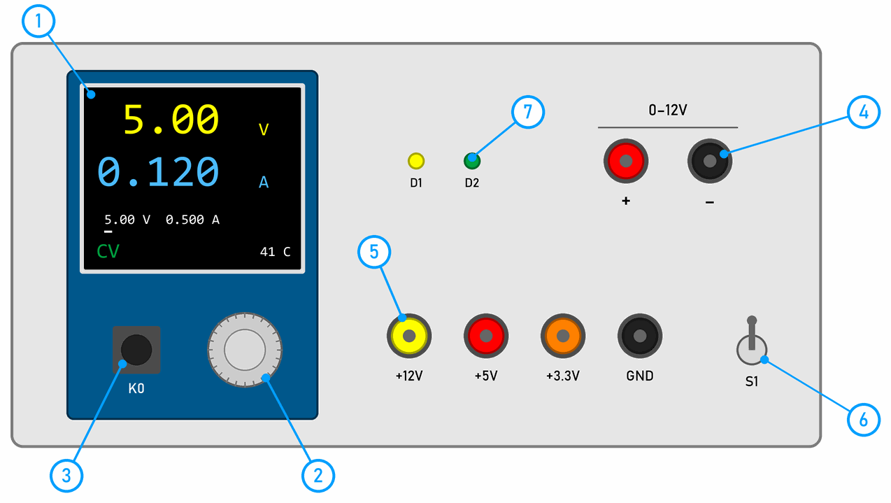
The numbers are the same as in the picture:
- The display (module U8): at the top are the measured voltage (yellow) and current (blue), and below them the set voltage and current limit, with a line under the digit the encoder changes. At the bottom it shows whether the output works as a constant voltage (CV) or constant current (CC) source, and the heat sink’s temperature.
- The encoder: turning it changes the digit above the line, and pressing it moves to the next digit: ones, tenths and hundredths of a volt, then tenths, hundredths and thousandths of an amp.
- Button K0 switches the adjustable output on and off. When the supply is switched on, the output is always off.
- The adjustable output: the red terminal is +, the black one −.
- The fixed outputs: +12 V, +5 V, +3.3 V and GND. The terminals have the colours of the ATX supply’s wires: yellow, red, orange and black.
- Switch S1 switches the whole supply on and off.
- The LEDs: the yellow D1 is on as soon as the supply is plugged in, and the green D2 while it is switched on.
The display, the encoder and button K0 are on one ready-made module. It has a 2.0" display (240 × 320, ST7789 chip). The same module also comes with a 1.8" display (128 × 160, ST7735), and the program works with both.
How it fits together
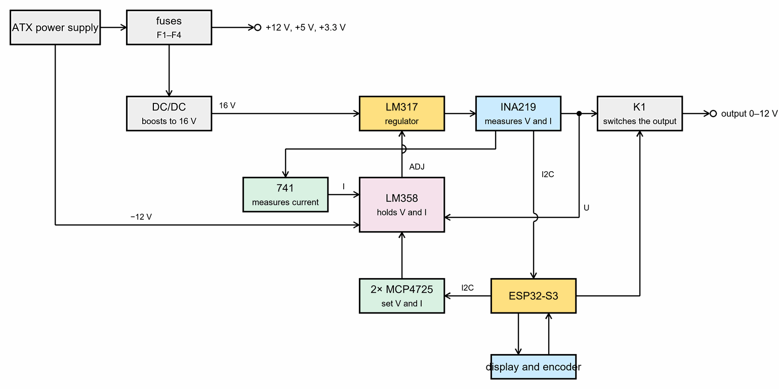
The supply has three parts, and each has its own schematic:
- The ATX supply with its fuses gives the fixed outputs and powers the other two parts.
- The adjustable output: a boost converter raises 12 V to 16 V, and the LM317 regulator turns that into the voltage we set. The regulator’s ADJ pin is controlled by the two operational amplifiers in an LM358 chip: one watches the voltage and the other the current.
- The control: the ESP32 reads the encoder, sends the set values to the operational amplifiers through two MCP4725 converters, reads the measured values from an INA219 module and shows them on the display. It switches the output on and off with relay K1.
How to read a block diagram is explained on the diagrams page.
The whole supply is also drawn as one schematic in KiCad, with every part from the parts list and every connection between them. You can download the schematic as a PDF or the KiCad project (a ZIP), which opens in KiCad 10 or newer.
The ATX power supply
Everything this supply needs comes from an old computer power supply (ATX). ATX is a standard that sets a computer power supply’s size, its voltages, wire colours and connectors, so all ATX supplies are alike, whoever made them. The same supply also powers the pinball machine.
We never open the supply
There are 230 V inside the supply, and its big capacitors stay charged to more than 300 V long after it is unplugged. A supply with a damaged case, one that smells burnt or one whose fan doesn't turn goes to electronic waste. Some older supplies have a red 115/230 V switch at the back: before switching on for the first time, check that it is set to 230.
How it works
The 230 V alternating voltage from the socket goes into the supply. The supply first rectifies and smooths it, as on the Rectifiers and voltage regulators page, which gives about 325 V of direct voltage inside it. From that, two converters make the low voltages. They work much like the buck converter on the Powering a project page, but they have a transformer, which separates the low voltages from the mains:
- a small converter runs as soon as the supply is plugged in, and gives only +5VSB, 5 V on standby,
- the main converter gives +12 V, +5 V, +3.3 V and −12 V, but only while the PS_ON signal keeps it on.
The converters switch on and off tens of thousands of times a second, so their transformer is much smaller than it would be for the 50 Hz from the socket.
The 24-pin connector
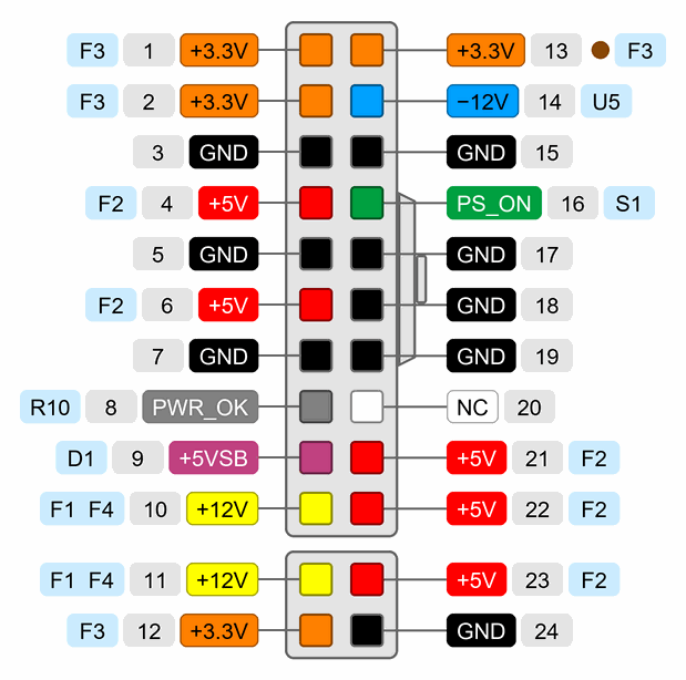
The supply connects to the motherboard with its main connector, 24 pins in two rows. The drawing shows it from the front, from the side with the holes, with the latch on the right. Each pin has its wire’s colour, and the blue labels show the part of this supply it is connected to. The ATX breakout board joins all the pins with the same voltage, so the circuit gets them together.
| Pins | Wire | Signal | What it is | In this supply |
|---|---|---|---|---|
| 10, 11 | yellow | +12 V | the computer’s main voltage, for the processor, graphics card, drives and fans | fixed output through F1, converter U1 through F4 |
| 4, 6, 21, 22, 23 | red | +5 V | for USB and older parts of the computer | fixed output through F2, and after it the ESP32, the display and the relay |
| 1, 2, 12, 13 | orange | +3.3 V | for the chips on the motherboard and the cards | fixed output through F3 |
| 14 | blue | −12 V | a voltage below GND, once for the computer’s serial ports; gives a small current | powers op-amp U5 |
| 3, 5, 7, 15, 17, 18, 19, 24 | black | GND | the common wire of all the voltages (COM in the ATX standard) | GND of the whole circuit |
| 9 | purple | +5VSB | 5 V on standby, on as soon as the supply is plugged in | yellow LED D1 |
| 16 | green | PS_ON | while it is joined to GND, the main converter runs | switch S1 |
| 8 | grey | PWR_OK | reports that all the voltages are all right | the ESP32 through R10 and R11 |
| 20 | – | – | empty, once −5 V on a white wire | – |
- A brown wire goes into pin 13 with the orange one (the brown dot in the drawing). Through it the supply measures the 3.3 V at the connector itself, and raises it if some of the voltage is lost in the wires.
- Pins 11, 12, 23 and 24 are a detachable part on many supplies, so the connector also fits older 20-pin motherboards.
- Each pin takes about 6 A. +12 V has two pins, so up to about 12 A, and this supply needs at most 8 A through F1 and F4.
- The supply’s other connectors (for the processor, the graphics card and the drives) have only +12 V, +5 V, +3.3 V and GND. The main connector is all this supply needs.
Voltages and currents
How much current the supply can give on each voltage is written on the label on its side. On +12 V, +5 V, +3.3 V and +5VSB, ATX allows the voltage to be up to 5 % off (on +12 V from 11.4 to 12.6 V), and on −12 V up to 10 % (from −10.8 to −13.2 V). This supply needs:
- +12 V: up to 5 A at the fixed output and up to 3 A for converter U1, up to 8 A in all,
- +5 V: up to 5 A, of which the ESP32, the display and the relay take about 0.2 A,
- +3.3 V: up to 3 A,
- −12 V: up to about 10 mA for the LM358,
- +5VSB: only LED D1, less than 10 mA.
That is up to about 130 W in all, so even an old 300 W supply is enough, if it gives at least 10 A on +12 V. Some supplies have two 12 V lines, +12V1 and +12V2, each with its own limit on the label. The main connector is on one of them, so that is the one to look at.
Switching on and off
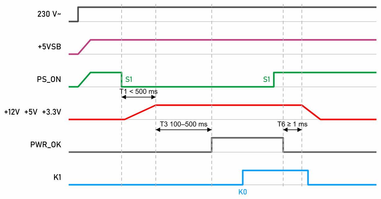
In the drawing time runs from left to right, but not to scale. When the supply is plugged in, +5VSB comes on at once and the yellow LED D1 lights. PS_ON is then at about 5 V, because a resistor in the supply pulls it up to +5VSB, so the main converter stays off.
- Switching on: when S1 joins PS_ON to GND, the main converter starts, and +12 V, +5 V and +3.3 V reach their values in less than half a second (T1 in the drawing). Only about 1 mA flows through S1.
- PWR_OK stays at 0 V for another 0.1 to 0.5 s (T3), until the voltages settle, and only then goes to about 5 V. In a computer, the motherboard holds the processor in reset during that time. In this supply, the ESP32 doesn’t let the output switch on until then: the display shows PWR_OK, and K0 does nothing. PWR_OK gives only a weak current, so divider R10 and R11 takes just 0.14 mA from it.
- The output switches on only when we press K0, and relay K1 connects the output.
- Switching off: when S1 separates PS_ON from GND, PWR_OK falls to 0 V at least 1 ms before the voltages start to fall (T6). The same happens when the 230 V goes away: PWR_OK stays for at least another 16 ms, and the voltages at least 1 ms longer. The ESP32 and the relay’s coil run on +5 V, so they switch off with it, and the relay lets go and switches the output off. When we switch the supply on again, the output stays off until we press K0.
The supply’s own protection
An ATX supply protects itself from too much current, a short circuit and too high a voltage. When too much current flows on one of its voltages, on most supplies only at 20 A or more, or when a voltage rises too high (on +12 V above 13.4 to 15.6 V), the supply switches off and stays off. It only runs again when we switch S1 off and on, or unplug it for a few seconds. The ESP32 switches off too, and the output stays off.
A current of 20 A would melt a thin wire or terminal before the supply switches off. That’s why each output also has its own fuse, as explained in the Fuses section. With a short circuit at a fixed output, either the fuse blows or the whole supply switches off, whichever is faster.
The ATX part of the circuit
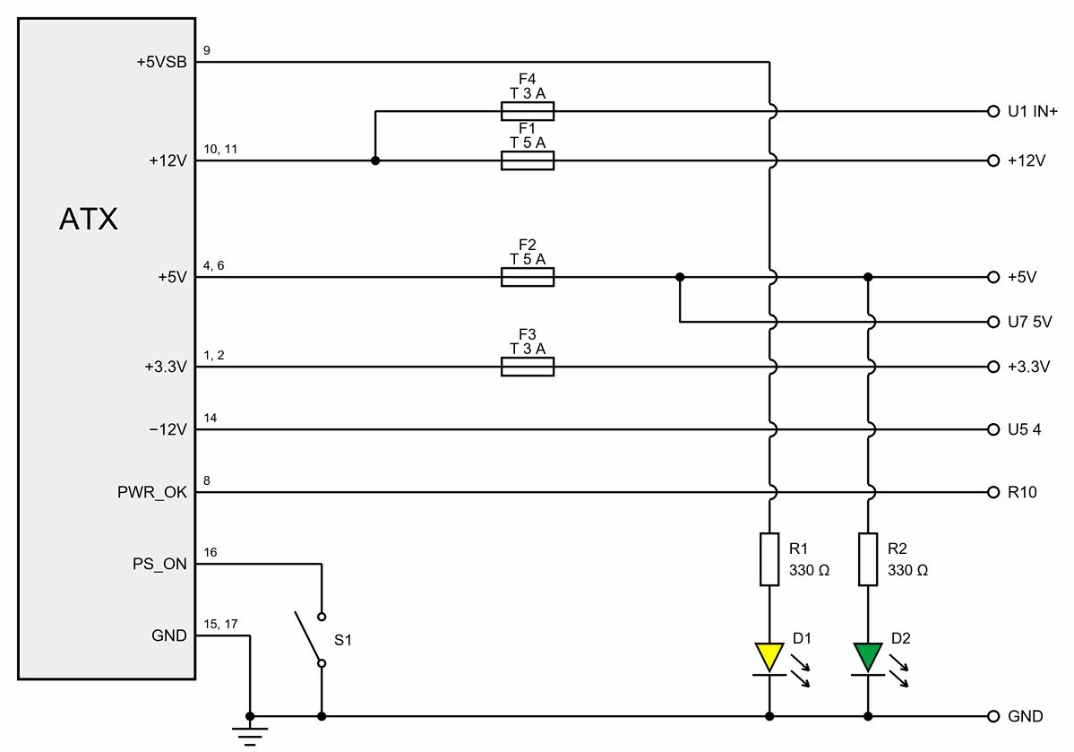
We switch the ATX supply on without a motherboard, just as on the pinball machine: switch S1 joins the green PS_ON wire (pin 16) to GND, and LEDs D1 and D2 show whether the supply is plugged in and whether it is on. How that works is explained in the Switching on and off section.
This project needs two more wires:
- −12 V (blue, pin 14) powers the operational amplifiers, so they can bring the output all the way down to 0 V.
- PWR_OK (grey, pin 8) is at about 5 V while all the supply’s voltages are all right. The ESP32 reads it and switches the output on only while it has voltage on it.
We don’t cut the supply’s connector, but use an ATX breakout board with screw terminals that also has −12 V and PWR_OK. Before building, check with a multimeter that the supply really gives about −12 V on the blue wire.
Fuses
An ATX supply can give 20 A or more on +12 V and +5 V, and only switches itself off at an even higher current. That much current can melt a thin wire or a terminal, so each output has its own fuse:
- F1 (5 A): the fixed +12 V output,
- F2 (5 A): the fixed +5 V output, and after it also the ESP32 and the relay,
- F3 (3 A): the fixed +3.3 V output,
- F4 (3 A): the adjustable output, at the input of the boost converter.
They are all slow-blow fuses (marked T), in holders for 5 × 20 mm fuses. The wires from the supply to the fuses and terminals are at least 0.75 mm², because up to 5 A flows through them. Why the thickness of a wire depends on the current is explained on the Wires, cables and connectors page.
Older ATX supplies need a minimum load to run steadily. The ESP32, the display and the LEDs always draw about 0.2 A on +5 V, which isn’t enough for some supplies. If the supply doesn’t switch on, or keeps switching off and on, we add a 22 Ω, 5 W resistor on +5 V, as on the pinball machine.
The adjustable output
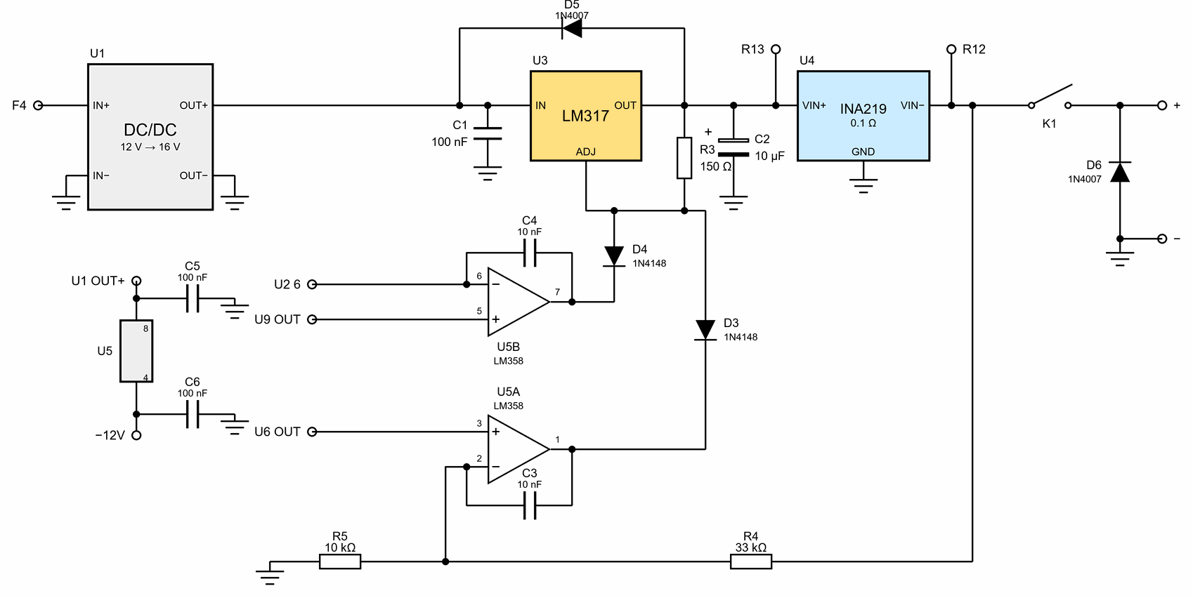
The heart of the adjustable output is the LM317 voltage regulator (U3). In front of it is a converter that gives it a high enough voltage, and its ADJ pin is controlled by two operational amplifiers.
The LM317 regulator
The LM317 is the adjustable version of the 78xx regulators on the Rectifiers and voltage regulators page. It has three pins: the input (IN), the output (OUT) and the adjust pin (ADJ). The regulator does only one thing: it keeps the output 1.25 V above the ADJ pin.
Resistor R3 of 150 Ω is between OUT and ADJ, so it also has 1.25 V across it, and a steady 8.3 mA flows through it. That current flows into the ADJ node and lifts it, and the output with it. The operational amplifiers take this current away through diodes D3 and D4 and so pull ADJ down: the lower they pull it, the lower the output voltage. The amplifiers get −12 V, so they can pull ADJ down to −1.25 V, and then the output is at 0 V.
R3 has one more job: the LM317 only works properly while at least a few milliamps flow through it, even when nothing is connected to the output.
LM317 pinout
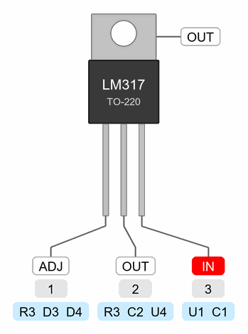
We look at the LM317 from the front, the side with the writing, with its leads pointing down.
- 1 ADJ (adjust): R3 lifts it from the output, and D3 and D4 pull it down.
- 2 OUT (output): goes to C2 and the INA219 module. The metal tab at the back is joined to it too, so without an insulating pad the heat sink would be at the output voltage as well.
- 3 IN (input): 16 V from converter U1, with C1 right next to the pin.
The XL6019 boost converter
The LM317 needs at least about 2 V more at its input than it gives at its output, and the INA219 module’s resistor, across which we measure the current, takes another 0.1 V at 1 A. If the LM317 got 12 V directly, we would get at most about 9.9 V at the output.
That’s why U1 is in front of it: a ready-made boost converter, which makes 16 V from 12 V. It works the other way round from the buck converter on the Powering a project page: it raises the voltage instead of lowering it. We use a module with an XL6019 chip, which takes up to 5 A at its input, so it gives the 16 W this supply needs (about 1.5 A from 12 V) with ease. We set the module’s output to 16.0 V with its potentiometer, before connecting it to the rest of the circuit. The module can give up to 40 V, but we never set it above 16.5 V: the LM358 gets the module’s voltage and the −12 V, which may be as much as −13.2 V, and it may get at most 30 V in all. With 16 V the output reaches up to 13.9 V at 1 A, and the program allows at most 12 V.
XL6019 pinout
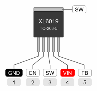
The chip is soldered onto the module, and the module has the IN+, IN−, OUT+ and OUT− terminals, so we don't connect its pins ourselves. This is what the module does with them:
- 1 GND: the common GND of the input and the output (IN− and OUT− are joined on the module).
- 2 EN (enable): switched on by the module, so the chip runs as soon as it gets power.
- 3 SW (switch): connects the module's coil to GND 180,000 times a second. The metal tab is joined to it too.
- 4 VIN (input): 12 V from F4, 5 to 40 V.
- 5 FB (feedback): the chip keeps 1.25 V on it. It gets it from a divider at the output, and the potentiometer changes the divider, and with it the output voltage.
Measuring the current: amplifier U2
The output current is measured by difference amplifier U2, a 741 operational amplifier with four resistors. It measures the voltage across the 0.1 Ω resistor on the INA219 module (U4), which all of the output current flows through, giving 0.1 V per amp across it. The amplifier makes that voltage 10 times bigger and gives 1 V for every amp, which is what amplifier U5B expects.
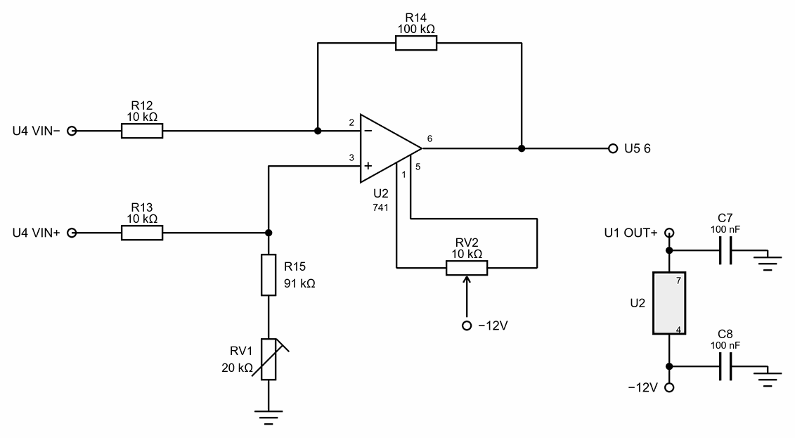
A difference amplifier subtracts the voltage on one side of the resistor from the voltage on the other side, and makes the difference as many times bigger as R14 is bigger than R12:
- Both sides of the resistor are at the output voltage, 0 to 12 V, and the difference between them is only 0.1 V per amp. The amplifier has to amplify that small difference and ignore the output voltage itself. It does that only when the ratio of the resistors at the + input equals the ratio at the − input: (R15 + RV1) / R13 = R14 / R12.
- 1 % resistors can be so far off that with 12 V at the output the amplifier would show up to 0.43 A even with no current. That’s why R15 has a trimmer RV1, a small adjustable resistor, next to it: with it we make the ratios equal once, as described in step 4 of Building and checking.
- The 741 itself can be up to 6 mV off, which would move the current by up to 66 mA. That’s why it has pins 1 and 5 for offset nulling: a 10 kΩ trimmer RV2 between them, with its wiper on −12 V, cancels that error. We adjust it in step 4 too. After that, only a small error is left when the chip warms up.
- The amplifier’s inputs are at about 12.6 V at the highest output voltage. On a 741 they may go up to 3 V below its supply, so up to 13 V.
- The current through R3 (8.3 mA) isn’t seen by the amplifier, because it flows before the resistor. So the current limit applies to the current the circuit at the output gets.
741 pinout
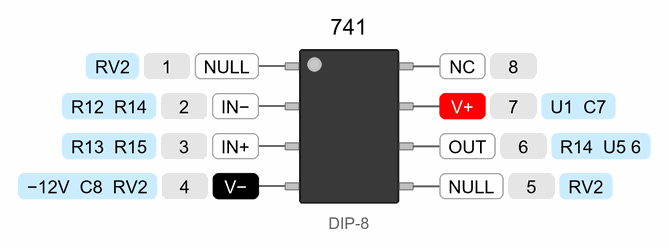
The 741 is a single operational amplifier in a DIP-8 package, sold as the µA741, UA741 or LM741. We look at it from above, with the notch or dot by pin 1 at the top left.
- 2 IN−: through R12 from the side of the resistor towards the output, and through R14 from the amplifier's output.
- 3 IN+: through R13 from the side of the resistor towards the LM317, and R15 and RV1 connect it to GND.
- 6 OUT (output): 1 V per amp, to pin 6 of U5 and back through R14.
- 7 V+: 16 V from U1, with C7.
- 4 V−: −12 V, with C8 and the wiper of trimmer RV2.
- 1 and 5 NULL: the ends of trimmer RV2, which cancels the amplifier's error.
- 8 NC: not connected inside the chip.
The LM358 operational amplifier
The LM358 chip (U5) holds two identical operational amplifiers, U5A and U5B, with a shared supply. Pin 8 (V+) gets 16 V from converter U1, and pin 4 (V−) −12 V from the ATX supply. That’s 28 V between them, and the LM358 may get at most 30 V. That’s why we never set converter U1 above 16.5 V. Capacitors C5 and C6 (100 nF) sit next to the two supply pins.
LM358 pinout
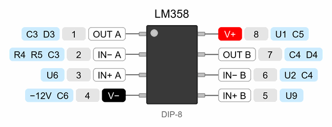
We look at the LM358 from above, with the notch or dot by pin 1 at the top left. The pins are counted around the chip, anticlockwise.
- 1, 2, 3: amplifier U5A, which holds the voltage. Its output (1) pulls ADJ through D3, its − input (2) gets the voltage from divider R4 and R5, and its + input (3) the set voltage from U6.
- 5, 6, 7: amplifier U5B, which holds the current. Its + input (5) gets the current limit from U9, its − input (6) the voltage from amplifier U2, and its output (7) pulls ADJ through D4.
- 4 V−: −12 V, with C6.
- 8 V+: 16 V from U1, with C5.
Voltage: amplifier U5A
An operational amplifier compares the voltages at its two inputs and changes its output until they are equal. U5A gets the set voltage from an MCP4725 converter (U6), from 0 to 3.3 V, at its + input. At its − input it gets the output voltage made smaller by a voltage divider of resistors R4 (33 kΩ) and R5 (10 kΩ). When the output voltage is too high, U5A lowers its output and pulls ADJ down through D3. When it is too low, U5A raises its output, D3 stops conducting and R3 lifts ADJ. So the output settles at:
The MCP4725 has 4096 steps, so one step of the output voltage is 3.5 mV. The highest 14.19 V is more than the 12 V we need, so the output reaches 12 V even when the 3.3 V is 2 % lower. The divider measures the voltage after the INA219 module, so U5A also makes up for the 0.1 V its resistor takes. Capacitor C3 slows the amplifier down a little, so that the loop doesn’t oscillate.
Current: amplifier U5B
U5B compares the voltage from amplifier U2, 1 V per amp, with the set limit from an MCP4725 converter (U9). While the current is lower, U5B keeps its output high and D4 doesn’t conduct. When the current reaches the limit, U5B pulls ADJ down through D4, just enough to keep the current at the limit.
Both amplifiers can only pull ADJ down, and the one that wants it lower wins. While the circuit at the output draws less than the limit, U5A holds the voltage and the output works as a constant voltage source (CV). If the current would go over the limit, U5B takes over and the output works as a constant current source (CC): the voltage drops just enough to keep the current at the limit.
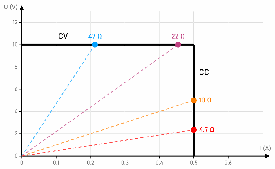
The graph shows this with 10 V and 0.5 A set. A 47 Ω resistor draws 0.213 A at 10 V, and a 22 Ω one 0.455 A: both are below the limit, so they get the full 10 V. A 10 Ω resistor would draw 1 A at 10 V, so the supply holds it at 0.5 A, and the voltage drops to 5 V. A 4.7 Ω one gets 2.35 V and a short circuit 0 V, always at 0.5 A.
A few more details:
- The current through divider R4 and R5 and through R12 (up to 0.4 mA at 12 V) flows through the INA219 module’s resistor, but not through the circuit at the output. So the program adds it to the set limit: 0.032 mA for every volt of the set voltage.
- The limit is fast, because a circuit does it, not the program. Behind it are the LM317’s own limit at about 1.5 to 2.2 A and fuse F4.
- Accuracy: the LM358 can be up to 7 mV off, so the voltage can be up to 30 mV off and the current up to 7 mA, plus the small error amplifier U2 has left after adjusting. The 3.3 V that the MCP4725 converters compare the set values with is a bigger source of error: if it is 2 % low, the output voltage and current are 2 % low too, and 12 V becomes 11.76 V. So we measure it and write it into the program. The display always shows the true value, and we correct the other steady errors in the program.
We try every new circuit with a limit of 0.1 A or less: if there is a mistake in it, no current big enough to destroy an LED or a transistor can flow. We raise the limit only when the circuit works and needs more current, for example for a motor.
Relay K1
The contact of relay K1 connects the output to the + terminal. The ESP32 switches it on only when we press K0, and off when we press K0 again or when something is wrong. The regulation keeps running while K1 is off, so the voltage is ready when we switch it on.
Heat
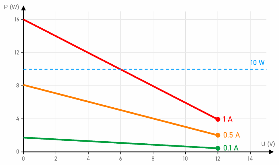
The LM317 is a linear regulator: all the voltage it doesn’t let through to the output it turns into heat. The power it turns into heat is the difference between the input and output voltages times the current. The lower the output voltage and the higher the current, the hotter the LM317 gets:
| Output | Current | Heat in the LM317 |
|---|---|---|
| 12 V | 1 A | 3.9 W |
| 5 V | 1 A | 11 W |
| 5 V | 0.5 A | 5.6 W |
| 0 V (short circuit) | 1 A | 16 W |
| 0 V (short circuit) | 0.1 A | 1.7 W |
That’s why the LM317 sits on a big aluminium heat sink. For 11 W the heat sink may have a thermal resistance of at most 3.7 K/W (it is in its data), which is a finned heat sink of about 100 × 60 × 30 mm. When the output is shorted for a long time at 1 A, the heat sink keeps getting hotter. So thermistor RT1 sits on it, and the program switches the output off when the heat sink reaches 80 °C and lets it be switched on again only once it has cooled below 70 °C. Behind that is the LM317’s own protection: it switches itself off when it overheats.
The metal tab on the back of the LM317 is connected to its output. So we insulate it from the heat sink with a silicone pad and a plastic bush around the screw. The heat sink gets hot enough to burn, so we put it on the back of the box, or inside it next to air vents.
Protection diodes and capacitors
- C1 (100 nF) sits right at the LM317’s input, and C2 (10 µF) at its output. With them the LM317 runs steadily and doesn’t oscillate. C5 and C6 (100 nF) sit right at the LM358’s supply pins.
- C2 isn’t bigger on purpose. A big capacitor at the output would discharge with a high current into a short circuit, and the current limit can’t stop that, because it is in front of it.
- D5 protects the LM317 when the input voltage falls faster than the output, for example when F4 blows. C2 then discharges through D5, not backwards through the LM317.
- D6 protects the supply when someone connects a battery or another supply to the output the wrong way round: the current then flows through D6, not through the LM317 and the measuring modules.
The control
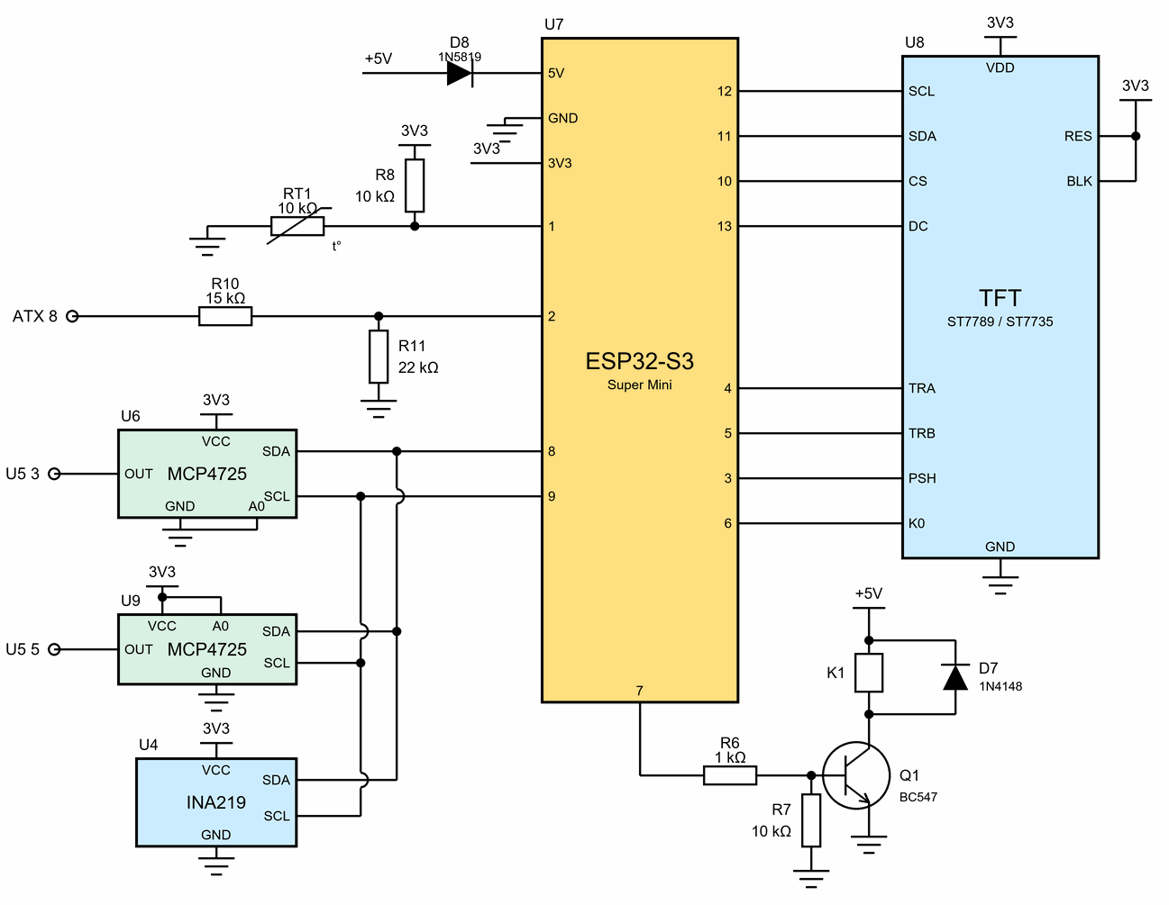
The control is run by an ESP32-S3 Super Mini (U7), an ESP32-S3 18 × 23.5 mm in size. Its pinout is on the ESP32 and ESP8266 page. It gets +5 V after fuse F2 through diode D8, and its 3.3 V (3V3) powers the display module, both MCP4725 converters, the INA219 and the thermistor. What is on each pin:
| ESP32 pin | Connected to | What it does |
|---|---|---|
| 12, 11, 10, 13 | the display’s SCL, SDA, CS, DC | SPI link to the display |
| 4, 5 | TRA, TRB | the encoder |
| 3, 6 | PSH, K0 | the encoder’s button and button K0 |
| 8, 9 | SDA, SCL | I2C: MCP4725 and INA219 |
| 7 | R6, Q1 | relay K1 |
| 2 | R10, R11 | PWR_OK from the ATX supply |
| 1 | R8, RT1 | the heat sink’s temperature |
| 3V3 | the display’s RES, BLK | the display is reset by a command, and the backlight is always on |
The Super Mini has pins 1 to 13 on its edges, plus TX and RX; the others are small pads on the underside, which are hard to solder wires to. So we use only the pins on the edges, and connect the display’s RES and BLK straight to 3V3. Pin 1 is on the analog-to-digital converter ADC1, as are the pins up to 10, so it can measure the thermistor’s voltage. The ESP32-S3 checks pin 3 when it starts only if it was set up that way in the factory, and it only has the encoder’s button on it anyway. We don’t use pins 0, 45 and 46, which decide how the ESP32-S3 starts, nor 19 and 20 (USB) or 48 (the LED on the Super Mini). Why is explained on the ESP32 and ESP8266 page.
- Relay K1 draws about 70 mA, too much for an ESP32 pin, so transistor Q1 switches it. R7 keeps Q1 off while the ESP32 starts, so the output can’t switch on by itself. Diode D7 takes over the coil’s current when the relay switches off.
- RT1 is a 10 kΩ thermistor (NTC, B = 3950) stuck to the heat sink. With resistor R8 it makes a divider, so the voltage on pin 1 falls as the heat sink warms up.
- R10 and R11 turn the 5 V on PWR_OK into about 3 V, which is as much as an ESP32 pin may get.
- D8 is a Schottky diode. When the Super Mini is plugged into a computer with a USB cable, D8 keeps the computer’s 5 V out of the ATX supply and everything else on +5 V. About 0.3 V is lost across it, which doesn’t bother the Super Mini’s 3.3 V regulator.
The MCP4725 converters
The MCP4725 is a digital-to-analog converter with one output and 12 bits (4096 steps). We have two: U6 sets the voltage and U9 the current limit. Its output goes from 0 to its supply voltage, so both are powered with 3.3 V from the ESP32. They must not run on 5 V, because the I2C resistors on the modules are connected to the module’s supply, and the ESP32’s pins must not get 5 V.
- The A0 pin sets the converter’s address: U6 is at 0x60 (A0 on GND) and U9 at 0x61 (A0 on 3V3). On some modules the addresses are 0x62 and 0x63; then we change them in the program.
- When it is switched on, the converter puts the value saved in its memory on its output, so the program saves a zero in both.
MCP4725 pinout
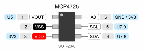
The chip is on the module, and the module has the pins VCC, GND, SCL, SDA, A0 and OUT. Not every maker puts them in the same order, so read the labels.
- 1 VOUT (output, OUT on the module): 0 to 3.3 V. On U6 it goes to pin 3 of U5, on U9 to pin 5.
- 2 VSS: GND.
- 3 VDD (VCC on the module): 3V3 from the ESP32. It is also the reference, so the accuracy depends on it.
- 4 SDA and 5 SCL: the I2C link, to pins 8 and 9 of the ESP32.
- 6 A0: the address, on GND for U6 and on 3V3 for U9.
Measuring the output: INA219
The INA219 module (U4) measures the voltage and current at the output for the display. It measures the current across its 0.1 Ω resistor, and the voltage from its IN− pin to GND, up to 26 V. The ESP32 reads both over I2C. Amplifier U2 measures the current for the regulation across the same resistor. Both MCP4725s and the INA219 share one I2C link, at addresses 0x60, 0x61 and 0x40, as on the How devices talk page.
INA219 pinout
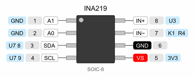
The chip is on the module, and the module has the pins VCC, GND, SCL, SDA, VIN+ and VIN−. The drawing shows the SOIC-8 package; the INA219 in a SOT-23-8 package has the same pins under other numbers.
- 1 A1 and 2 A0: the address. They are on GND on the module, so the address is 0x40.
- 3 SDA and 4 SCL: the I2C link, to pins 8 and 9 of the ESP32.
- 5 VS (VCC on the module): a 3 to 5.5 V supply, here 3V3.
- 6 GND.
- 7 IN−: the side of the resistor towards the output, to relay K1 and divider R4. It also measures the voltage from this pin to GND.
- 8 IN+: the side of the resistor towards the LM317.
The display module
The display module (U8) holds the colour display, the encoder and button K0. The display has its own controller chip, the ST7789 (or the ST7735 on the 1.8" display), which is built into the display itself, so we can’t reach its pins. The ESP32 talks to it over SPI, and the encoder and the button are just contacts to GND.
Display module pins
The order of the pins depends on the module, so read the labels.
- VDD and GND: the supply, 3V3 from the ESP32.
- SCL, SDA, CS and DC: the SPI link to the display (clock, data, chip select, command or data), to pins 12, 11, 10 and 13 of the ESP32. Even though they are called SCL and SDA, this is not an I2C link.
- RES (reset) and BLK (backlight): to 3V3.
- TRA and TRB: the encoder's two contacts, to pins 4 and 5.
- PSH: the encoder's button, to pin 3.
- K0: button K0, to pin 6.
The program
The program needs the ESP32 package and four libraries, which we install in the Arduino IDE (Library Manager): Adafruit ST7735 and ST7789 Library, Adafruit GFX Library, Adafruit MCP4725 and Adafruit INA219. If the module has a 1.8" display (ST7735), change USE_ST7789 to 0 in the program. For the Super Mini, choose the board ESP32S3 Dev Module in the Tools menu. If the program doesn’t upload the first time, hold the BOOT button, press and release RST, then release BOOT.
// Lab power supply: control and display (ESP32-S3 Super Mini)
// The encoder sets the voltage and the current limit, and K0 switches the output on and off.
// Two MCP4725s turn the set values into voltages for the control loop, and the INA219
// measures the voltage and current at the output.

#include <SPI.h>
#include <Wire.h>
#include <Preferences.h>
#include <Adafruit_GFX.h>
#include <Adafruit_ST7735.h>
#include <Adafruit_ST7789.h>
#include <Adafruit_MCP4725.h>
#include <Adafruit_INA219.h>

// Which display the module has: 1 = 2.0" ST7789 (240 x 320), 0 = 1.8" ST7735 (128 x 160)
#define USE_ST7789 1

// Pins (the display's RES and BLK are connected to 3V3)
const int PIN_SCK = 12, PIN_MOSI = 11, PIN_CS = 10, PIN_DC = 13;
const int PIN_ENC_A = 4, PIN_ENC_B = 5, PIN_ENC_SW = 3, PIN_K0 = 6;
const int PIN_SDA = 8, PIN_SCL = 9;
const int PIN_RELAY = 7, PIN_PWR_OK = 2, PIN_NTC = 1;

// The control loop
const float DAC_REF = 3.30;     // the ESP32's 3V3 measured with a multimeter: both DACs' reference
const float DIVIDER = (33.0 + 10.0) / 10.0;   // R4 and R5
const float V_FULL = DAC_REF * DIVIDER;       // output voltage at DAC code 4095 (14.19 V)
const float I_FULL = DAC_REF;   // U2 gives 1 V per amp, so code 4095 is 3.3 A
const uint8_t DAC_V_ADDR = 0x60, DAC_I_ADDR = 0x61;   // U6 (A0 on GND) and U9 (A0 on 3V3)
const float I_EXTRA = 0.0000323; // current our circuit takes after the shunt (R4, R5, R12), A per volt
const float V_MAX = 12.0;       // highest voltage you can set
const float I_MIN = 0.010, I_MAX = 1.000;   // lowest and highest current limit
const float TEMP_MAX = 80.0;    // heat sink temperature that switches the output off

#if USE_ST7789
Adafruit_ST7789 tft = Adafruit_ST7789(&SPI, PIN_CS, PIN_DC, -1);
#else
Adafruit_ST7735 tft = Adafruit_ST7735(&SPI, PIN_CS, PIN_DC, -1);
#endif
Adafruit_MCP4725 dacV, dacI;   // U6 sets the voltage, U9 the current limit
Adafruit_INA219 ina;
Preferences memory;

float setV = 5.0;          // set voltage, V
float setI = 0.100;        // set current limit, A
bool outputOn = false;
int cursor = 0;            // which digit the encoder changes: 0-2 voltage, 3-5 current
const float STEP[6] = {1.0, 0.1, 0.01, 0.1, 0.01, 0.001};
String fault = "";         // why the output can't be switched on ("" = all is well)
float volts = 0, amps = 0, temp = 0;
int s = 1;                 // text scale: 1 for the small display, 2 for the big one

struct Button {
  int pin;
  bool down;
  unsigned long changed;
};
Button encButton = {PIN_ENC_SW, false, 0};
Button k0Button = {PIN_K0, false, 0};

// --- the encoder ---------------------------------------------------------------------------
// Every change on A or B is looked up in a table of allowed steps. A bounce goes one step
// forward and one back, so it cancels itself out.
const int8_t ENC_TABLE[16] = {0, -1, 1, 0, 1, 0, 0, -1, -1, 0, 0, 1, 0, 1, -1, 0};
volatile int encCount = 0;
volatile uint8_t encState = 0;

void IRAM_ATTR encoderChanged() {
  encState = ((encState << 2) | (digitalRead(PIN_ENC_A) << 1) | digitalRead(PIN_ENC_B)) & 0x0F;
  encCount += ENC_TABLE[encState];
}

// True once, when the button is pressed (ignoring bounce shorter than 30 ms)
bool pressed(Button &b) {
  bool down = digitalRead(b.pin) == LOW;
  if (down != b.down && millis() - b.changed > 30) {
    b.down = down;
    b.changed = millis();
    return down;
  }
  return false;
}

// --- the output ------------------------------------------------------------------------------
void setOutput(bool on) {
  outputOn = on;
  digitalWrite(PIN_RELAY, on ? HIGH : LOW);
}

void setDac() {
  int codeV = constrain(lround(setV / V_FULL * 4095), 0, 4095);
  int codeI = constrain(lround((setI + setV * I_EXTRA) / I_FULL * 4095), 0, 4095);
  dacV.setVoltage(codeV, false);
  dacI.setVoltage(codeI, false);
}

float heatSinkTemp() {
  float mv = analogReadMilliVolts(PIN_NTC);                // NTC to GND, 10 kOhm to 3.3 V
  if (mv < 10 || mv > 3290) return 999;                    // wire broken or shorted
  float r = 10000.0 * mv / (3300.0 - mv);
  return 1.0 / (1.0 / 298.15 + log(r / 10000.0) / 3950.0) - 273.15;
}

// --- the display ------------------------------------------------------------------------------
void text(int x, int y, int size, uint16_t color, const char *str) {
  tft.setTextSize(size * s);
  tft.setTextColor(color, ST77XX_BLACK);   // with a background, so new text covers the old
  tft.setCursor(x * s, y * s);
  tft.print(str);
}

void drawScreen() {
  char buf[24];
  snprintf(buf, sizeof buf, "%5.2f", volts);
  text(4, 6, 3, ST77XX_YELLOW, buf);
  text(100, 20, 1, ST77XX_YELLOW, "V");
  snprintf(buf, sizeof buf, "%5.3f", amps);
  text(4, 40, 3, ST77XX_CYAN, buf);
  text(100, 54, 1, ST77XX_CYAN, "A");

  // the set values, with a line under the digit the encoder changes
  text(4, 80, 1, ST77XX_WHITE, "Set:");
  snprintf(buf, sizeof buf, "%5.2f V", setV);
  text(4, 92, 1, ST77XX_WHITE, buf);
  snprintf(buf, sizeof buf, "%5.3f A", setI);
  text(64, 92, 1, ST77XX_WHITE, buf);
  const int DIGIT_X[6] = {4 + 6, 4 + 18, 4 + 24, 64 + 12, 64 + 18, 64 + 24};
  tft.fillRect(0, 101 * s, tft.width(), 2 * s, ST77XX_BLACK);
  tft.fillRect(DIGIT_X[cursor] * s, 101 * s, 5 * s, 2 * s, ST77XX_WHITE);

  // the state of the output
  bool cc = outputOn && amps >= setI * 0.98 - 0.002;
  text(4, 112, 2, outputOn ? ST77XX_GREEN : ST77XX_RED, outputOn ? "ON " : "OFF");
  text(72, 112, 2, ST77XX_WHITE, outputOn ? (cc ? "CC" : "CV") : "  ");
  snprintf(buf, sizeof buf, "%3.0f C", temp);
  text(4, 136, 1, ST77XX_WHITE, buf);
  snprintf(buf, sizeof buf, "%-10s", fault.c_str());
  text(52, 136, 1, ST77XX_RED, buf);
}

// --- setup() and loop() -----------------------------------------------------------------------
void setup() {
  pinMode(PIN_RELAY, OUTPUT);
  setOutput(false);                        // first of all: the output is off
  pinMode(PIN_ENC_A, INPUT_PULLUP);
  pinMode(PIN_ENC_B, INPUT_PULLUP);
  pinMode(PIN_ENC_SW, INPUT_PULLUP);
  pinMode(PIN_K0, INPUT_PULLUP);
  pinMode(PIN_PWR_OK, INPUT);
  attachInterrupt(digitalPinToInterrupt(PIN_ENC_A), encoderChanged, CHANGE);
  attachInterrupt(digitalPinToInterrupt(PIN_ENC_B), encoderChanged, CHANGE);

  SPI.begin(PIN_SCK, -1, PIN_MOSI, PIN_CS);
#if USE_ST7789
  tft.init(240, 320);
  s = 2;
#else
  tft.initR(INITR_BLACKTAB);
#endif
  tft.fillScreen(ST77XX_BLACK);

  Wire.begin(PIN_SDA, PIN_SCL);
  if (!dacV.begin(DAC_V_ADDR) || !dacI.begin(DAC_I_ADDR)) {
    fault = "DAC?";
  } else if (!ina.begin()) {
    fault = "INA219?";
  } else {
    // 0 into each DAC's own memory, so after a power-up it starts at 0 V and 0 A
    dacV.setVoltage(0, true);
    dacI.setVoltage(0, true);
  }

  memory.begin("lab", false);              // the last set values, but never "output on"
  setV = memory.getFloat("v", 5.0);
  setI = memory.getFloat("i", 0.100);
  if (fault == "") setDac();
  drawScreen();
}

void loop() {
  bool changed = false;

  // the encoder changes the digit under the line
  noInterrupts();
  int steps = encCount / 4;                // an EC11 makes 4 steps per click
  encCount -= steps * 4;
  interrupts();
  if (steps != 0 && fault != "DAC?" && fault != "INA219?") {
    if (cursor < 3) {
      setV = constrain(setV + steps * STEP[cursor], 0.0, V_MAX);
      setV = round(setV * 100) / 100.0;
    } else {
      setI = constrain(setI + steps * STEP[cursor], I_MIN, I_MAX);
      setI = round(setI * 1000) / 1000.0;
    }
    setDac();
    changed = true;
  }
  if (pressed(encButton)) {                // pressing the encoder moves to the next digit
    cursor = (cursor + 1) % 6;
    changed = true;
  }
  if (pressed(k0Button)) {                 // K0 switches the output on and off
    if (outputOn) {
      setOutput(false);
    } else if (fault == "") {
      memory.putFloat("v", setV);
      memory.putFloat("i", setI);
      setOutput(true);
    }
    changed = true;
  }

  // measure five times a second and check that everything is all right
  static unsigned long lastMeasure = 0;
  if (millis() - lastMeasure >= 200) {
    lastMeasure = millis();
    volts = ina.getBusVoltage_V();
    amps = max(0.0f, ina.getCurrent_mA() / 1000.0f);
    temp = heatSinkTemp();
    if (fault != "DAC?" && fault != "INA219?") {
      if (digitalRead(PIN_PWR_OK) == LOW) fault = "PWR_OK";
      else if (temp > TEMP_MAX) fault = "TEMP";
      else if (fault == "TEMP" && temp > TEMP_MAX - 10) fault = "TEMP";   // wait until it cools down
      else fault = "";
    }
    if (fault != "" && outputOn) setOutput(false);
    changed = true;
  }

  if (changed) drawScreen();
}
- A safe start:
setup()switches the relay off first, and only then loads the set values from memory. The program remembers the set voltage and current (Preferences), but never switches the output on by itself. - The encoder has two contacts that close one after the other as it turns. Every change on pins 4 and 5 runs
encoderChanged(), which looks up inENC_TABLEwhether it was a step forward or backward. When a contact bounces, it makes a step forward and one back, so the bounce cancels itself out. setDac()turns the set voltage and current into numbers from 0 to 4095 for the MCP4725 converters. It addssetV * I_EXTRAto the current, the current that divider R4 and R5 and resistor R12 draw at the set voltage.- Five times a second the program measures the voltage, current and temperature, checks PWR_OK and draws the display. If something is wrong, it switches the output off and writes why on the display: PWR_OK, TEMP, DAC? or INA219?.
- The display isn’t cleared: new text is drawn over the old with a black background, so the numbers don’t flicker.
- No Wi-Fi: the supply doesn’t use a wireless link and doesn’t send any data.
Building and checking
We build and check the supply part by part, and measure every voltage with a multimeter first, before connecting the next part:
- The ATX part: connect S1, the LEDs, the fuses and the fixed outputs. Switch the supply on and measure +12 V, +5 V, +3.3 V, −12 V and PWR_OK (about 5 V).
- The converter: connect U1 to F4, with nothing at its output, and set it to 16.0 V with its potentiometer, never more than 16.5 V.
- The regulation without the ESP32: instead of the MCP4725 converters, connect the wipers of two 10 kΩ potentiometers to pins 3 and 5 of U5, with each potentiometer between the +3.3 V terminal and GND, so each gives 0 to 3.3 V. While the ESP32 isn’t connected, relay K1 is off, so in steps 3 to 5 we measure at the INA219 module’s VIN− pin, not at the + terminal. Turn the voltage potentiometer and watch the multimeter: the voltage must go from 0 to about 14 V.
- Adjusting amplifier U2: with nothing at the output, measure the voltage on pin 6 of U2 to GND with the multimeter. Set the output to 0 V and turn trimmer RV2 until it reads 0.00 V. Then set 12 V and turn trimmer RV1 until it reads 0.00 V again (before that it can also be negative). The two trimmers affect each other a little, so do both adjustments once more. If the voltage doesn’t change while you turn RV2, that 741 has no offset nulling (some newer ones don’t), and the error stays. Finally, set the current limit to about 0.1 A (0.1 V on pin 5 of U5) and connect the INA219 module’s VIN− to GND with the multimeter set to measure current (the 10A socket): it must show about 0.1 A.
- Does it oscillate: connect a 10 Ω, 10 W resistor to the INA219 module’s VIN− and watch the voltage with an oscilloscope while connecting and disconnecting the resistor. The voltage may jump briefly, but must settle within less than a millisecond. If it oscillates, make C3 and C4 bigger.
- The control: connect the ESP32, the display module, both MCP4725s and the INA219. Measure the voltage on the ESP32’s 3V3 pin with the multimeter, write it into
DAC_REFand upload the program. Compare the display with the multimeter at a few voltages and currents, and correct the remaining errors inDIVIDERandI_EXTRA. - The protections: switch S1 off while the output is on (the relay must switch off), and warm the thermistor with a hair dryer (the output must switch off at 80 °C).
The parts go on perfboard; soldering is explained on the Soldering page. If something doesn’t work, the Troubleshooting a circuit page helps.
Parts list
| Label | Part | Note |
|---|---|---|
| ATX power supply | an old computer power supply with −12 V | |
| ATX breakout board | with terminals for −12 V and PWR_OK | |
| S1 | switch | small, only a weak current flows through it |
| F1, F2 | fuse T 5 A | 5 × 20 mm, with a holder |
| F3, F4 | fuse T 3 A | 5 × 20 mm, with a holder |
| D1, D2 | 5 mm LED | yellow and green |
| R1, R2 | resistor 330 Ω | |
| U1 | boost converter XL6019 | a module up to 5 A, with an adjustable output |
| U2 | 741 | operational amplifier, DIP-8 package (µA741, UA741 or LM741) |
| U3 | LM317 regulator | TO-220 package |
| heat sink | at most 3.7 K/W, with an insulating pad and bush | |
| U4 | INA219 module | with a 0.1 Ω resistor |
| U5 | LM358 | two operational amplifiers, DIP-8 package |
| U6, U9 | MCP4725 module | 12 bits, with an A0 pin for the address |
| U7 | ESP32-S3 Super Mini | ESP32-S3FH4R2: 4 MB flash, 2 MB PSRAM |
| U8 | display module | 2.0" ST7789 (or 1.8" ST7735), with an encoder and a button |
| K1 | 5 V relay | contact at least 2 A |
| Q1 | transistor BC547 | NPN |
| R3 | resistor 150 Ω | |
| R4 | resistor 33 kΩ | 1 % |
| R5 | resistor 10 kΩ | 1 % |
| R6 | resistor 1 kΩ | |
| R7, R8 | resistor 10 kΩ | |
| R10 | resistor 15 kΩ | |
| R11 | resistor 22 kΩ | |
| R12, R13 | resistor 10 kΩ | 1 % |
| R14 | resistor 100 kΩ | 1 % |
| R15 | resistor 91 kΩ | 1 % |
| RV1 | trimmer 20 kΩ | multi-turn |
| RV2 | trimmer 10 kΩ | |
| RT1 | NTC thermistor 10 kΩ | B = 3950, to stick on the heat sink |
| D3, D4, D7 | diode 1N4148 | |
| D5, D6 | diode 1N4007 | |
| D8 | diode 1N5819 | Schottky |
| C1, C5 to C8 | capacitor 100 nF | ceramic |
| C2 | capacitor 10 µF | electrolytic, 25 V |
| C3, C4 | capacitor 10 nF | ceramic |
| 4 mm terminals | 2 red, 2 black, yellow, orange | |
| wire | 0.75 mm² for currents up to 5 A |
Safety
- The ATX supply stays closed. 230 V comes in only through its own cable.
- Every output has a fuse, so a short circuit on a fixed output blows the fuse, not a wire.
- The output never switches on by itself: after switching on, a restart or a fault, only button K0 switches it on.
- The heat sink gets hot and can burn. Don’t touch it while the supply is running at a high current.
- GND is earthed: in an ATX supply GND is connected to the metal case, and the case to the earth in the socket. So connect the ground clip of a mains-powered oscilloscope only to the supply’s GND.
- We don’t charge batteries with this supply, least of all LiPo batteries. They need chargers that watch the voltage of each cell, as the Batteries page explains.
What comes next
The supply hasn’t been built yet: the numbers on this page are calculated from the parts’ data. When we make the first one, we will measure the accuracy of the voltage and current, the heat sink’s temperature at 1 A, and how the loop settles when the load changes, and write them here.